Important Facts For Prelims
Design Linked Incentive (DLI) Scheme
- 07 Jan 2026
- 7 min read
Why in News?
India’s Design Linked Incentive (DLI) Scheme for Semiconductors has shown strong on-ground outcomes, highlighting rapid progress in building a self-reliant semiconductor design ecosystem amid global supply-chain vulnerabilities.
What are the Key Facts About the Design Linked Incentive (DLI) Scheme?
- About: The DLI Scheme is a central government initiative implemented by the Ministry of Electronics and Information Technology (MeitY) under the Semicon India Programme to promote indigenous semiconductor chip design by providing financial incentives and advanced design infrastructure to domestic startups and MSMEs.
- Objective: The DLI scheme aims to create a globally competitive, self-reliant chip design ecosystem focused on fabless semiconductor design.
- Fabless semiconductor design means designing and developing semiconductor chips without owning manufacturing plants, with fabrication outsourced to specialised foundries.
- Need for DLI Scheme: Fabless semiconductor companies occupy the most strategic position in the electronics value chain, as design and IP contribute over half of a chip’s value, account for up to 50% of value addition and 20–50% of the Bill of Materials, and drive nearly 30–35% of global semiconductor sales.
- Since design and IP determine performance, efficiency, security, and long-term competitiveness, the absence of indigenous design capabilities leaves countries dependent on imported core technologies even with local manufacturing, underscoring the need to build a strong domestic fabless ecosystem through the DLI Scheme.
- Eligibility The DLI Scheme covers startups (as per Department for Promotion of Industry and Internal Trade (DPIIT) notification, 2019), MSMEs (as per MSME notification, 2020), and domestic companies owned by resident Indian citizens in line with Foreign Direct Investment (FDI) Policy Circular, 2017 or extant norms.
- This inclusive design allows participation across stages of enterprise maturity.
- Scope of Support: Support is provided across the entire semiconductor design lifecycle, including Integrated Circuits (ICs), chipsets, Systems-on-Chip (SoCs), systems, and IP cores.
- The scheme emphasises indigenous design, IP ownership, and deployment in electronic products.
- Financial Incentives: The scheme offers two major incentives. The Product Design Linked Incentive reimburses up to 50% of eligible expenditure, capped at ₹15 crore per application.
- The Deployment Linked Incentive provides 4–6% of net sales turnover for five years, capped at Rs 30 crore, subject to minimum sales and successful product deployment.
- Design Infrastructure Support: Provided through the ChipIN Centre operated by Centre for Development of Advanced Computing (C-DAC).
- This includes access to advanced National EDA (Electronic Design Automation) Tool Grid, IP core repositories, MPW prototyping, and post-silicon validation, significantly lowering entry barriers for chip design.
- Key Achievements of DLI: Under the DLI scheme, 24 chip-design projects have been sanctioned across areas such as video surveillance, drone detection, energy meters, microprocessors, satellite communications, and broadband and Internet of Things System on a Chip (IoT SoC).
- The ChipIN Centre has democratised access to chip design infrastructure, supporting about 1 lakh engineers and students across 400 organisations, while the national EDA Grid has seen extensive usage, reflecting strong ecosystem adoption.
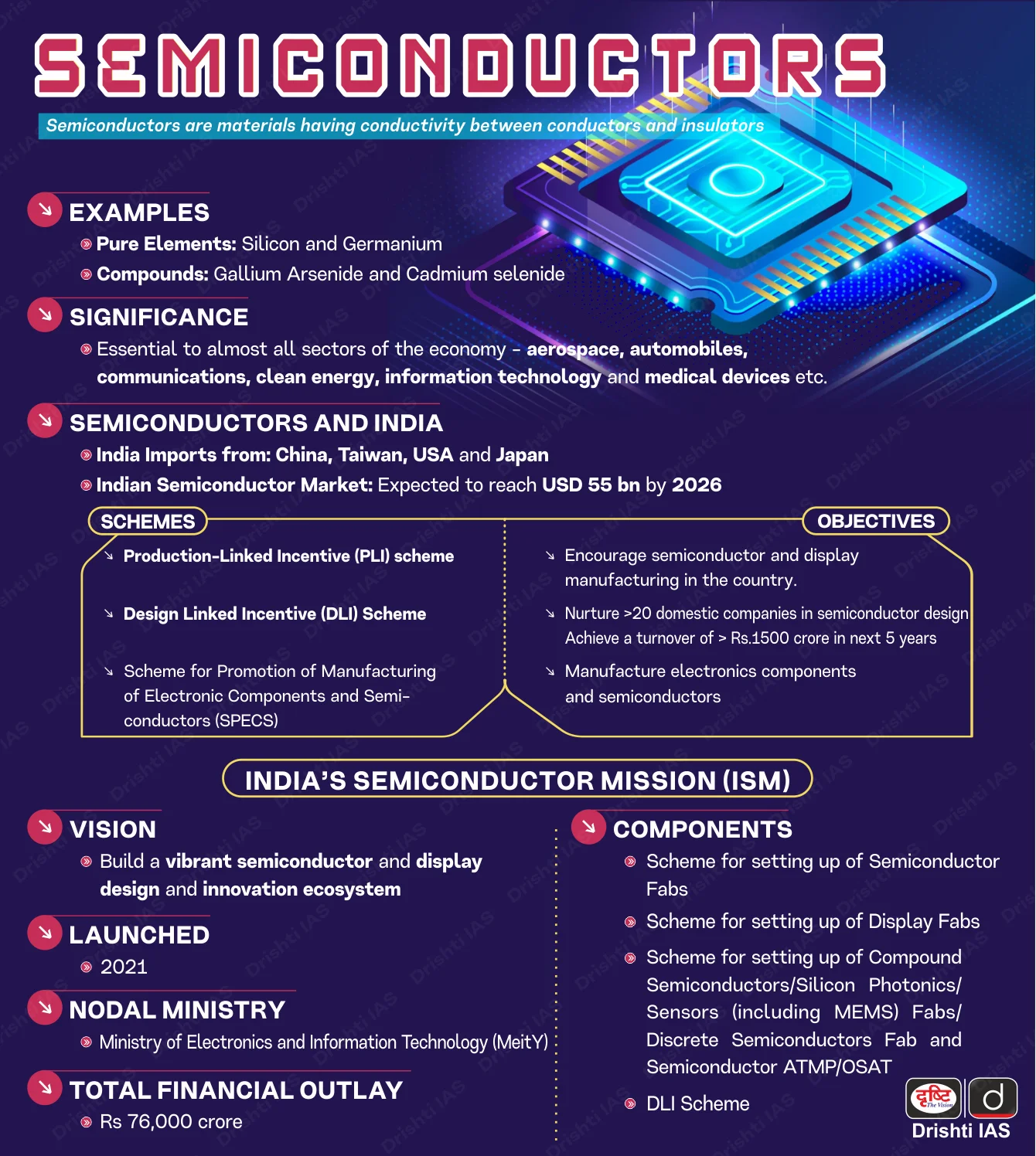
Key Institutional Frameworks for Semiconductor Design in India
- Semicon India Programme (SIM): With an outlay of Rs 76,000 crore, SIM supports semiconductor and display manufacturing as well as chip design.
- Centre for Development of Advanced Computing (C-DAC) acts as the nodal implementing agency.
- Chips to Startup (C2S) Programme: A national capacity-building initiative across academic institutions to create ~85,000 industry-ready professionals at BTech, MTech, and PhD levels in semiconductor chip design.
- Microprocessor Development Programme: Led by C-DAC, IIT Madras, and IIT Bombay, this programme has delivered open-source, indigenous microprocessors such as VEGA, SHAKTI, and AJIT, advancing technological self-reliance.
Frequently Asked Questions (FAQs)
1. What is the Design Linked Incentive (DLI) Scheme?
It is a central government scheme implemented by the Ministry of Electronics and Information Technology under the Semicon India Programme to promote indigenous semiconductor chip design via incentives and shared infrastructure.
2. Why is the DLI Scheme necessary for India?
Design and IP contribute over half of a chip’s value, up to 50% value addition, and 20–50% of BOM, while fabless firms drive ~30–35% of global sales—making indigenous design critical for competitiveness and security.
3. Who is eligible under the DLI Scheme?
Startups (DPIIT), MSMEs, and domestic companies owned by resident Indian citizens as per FDI norms, enabling participation across enterprise maturity.
UPSC Civil Services Examination, Previous Year Question (PYQ)
Prelims:
Q. Which one of the following laser types is used in a laser printer? (2008)
(a) Dye laser
(b) Gas laser
(c) Semiconductor laser
(d) Excimer laser
Ans: (c)
Mains
Q. India aims to become a semiconductor manufacturing hub. What are the challenges faced by the semiconductor industry in India? Mention the salient features of the India Semiconductor Mission. (2025)