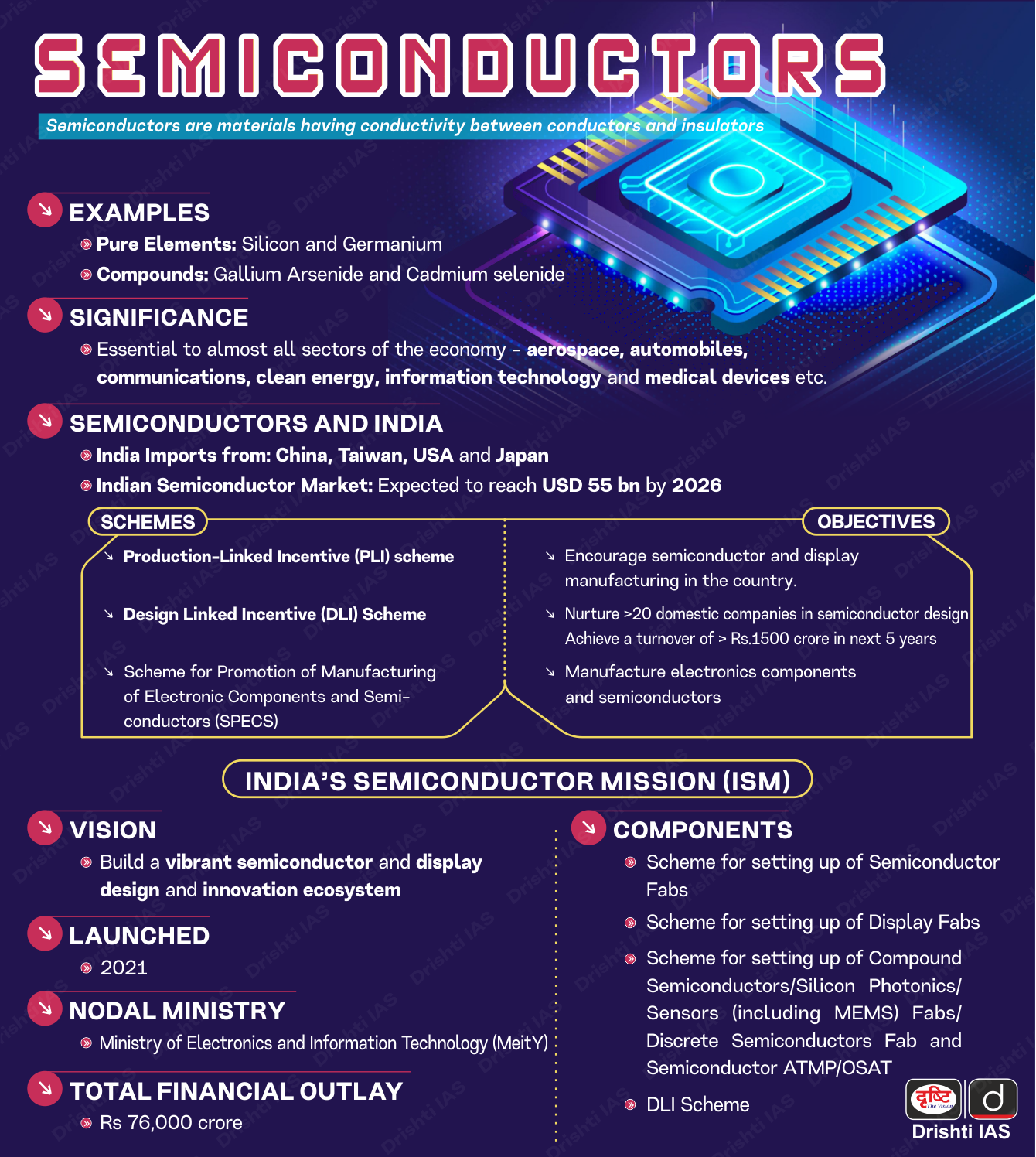
Important Facts For Prelims
Chips to Start-up (C2S) Programme
- 20 Jan 2026
- 5 min read
Why in News?
Recently, the Government has released performance outcomes of the Chips to Start-up (C2S) Programme, highlighting large enrolment, shared wafer runs, student-designed chips and patent generation.
What is the Chips to Start-up (C2S) Programme?
- About: The C2S Programme is an umbrella capacity-building initiative launched by the Ministry of Electronics and Information Technology (MeitY) in 2022, with a total outlay of ₹250 crore over five years, covering academic institutions across India.
- Target: The C2S Programme targets the development of 85,000 industry-ready professionals across undergraduate, postgraduate, and doctoral levels.
- Expansion: Beyond skill development, it seeks to incubate 25 start-ups, enable 10 technology transfers, provide access to SMART lab facilities, train one lakh students, generate 50 patents, and support at least 2,000 focused research publications.
- Impact: Through this integrated approach, the programme promotes innovation, enhances employability, strengthens the role of academic institutions in India’s semiconductor value chain, and lays a strong foundation for self-reliance and global competitiveness in the semiconductor sector.
- Programme Approach: The C2S Programme follows a comprehensive, hands-on model that integrates academic instruction with industry-led training, mentorship, and multi-year R&D projects.
- Through a coordinated institutional ecosystem involving academic institutions, the ChipIN Centre at C-DAC Bengaluru, and NIELIT SMART Labs, the programme provides shared infrastructure, centralized training, and end-to-end exposure to chip design, fabrication, and testing using advanced EDA tools and real-world semiconductor workflows, including ASICs, SoCs, and IP core development.
- Fabrication: Under the C2S Programme, the Centre aggregates student chip designs from participating institutions every quarter, verifies design compliance, and consolidates approved layouts onto shared wafers that are fabricated using 180 nm technology at the Semi-Conductor Laboratory (SCL), Mohali, followed by packaging and delivery of fabricated chips to students.
- Support: The ChipIN Centre also offers centralized technical support and handholding to participating institutions, resolving over 4,855 support requests, and enabling continuous design improvement and large-scale hands-on exposure to semiconductor fabrication and testing.
Frequently Asked Questions (FAQs)
1. What is the Chips to Start-up (C2S) Programme?
The C2S Programme is a MeitY initiative launched in 2022 to build semiconductor design capacity in Indian academic institutions and start-ups.
2. What are the main objectives of C2S?
The programme aims to train skilled semiconductor professionals, support start-ups and technology transfers, and promote patents and research in chip design.
3. What is the ChipIN Centre?
The ChipIN Centre at C-DAC Bengaluru is a national shared design facility providing tools, IP libraries, mentoring and fabrication aggregation.
UPSC Civil Services Examination, Previous Year Question (PYQ)
Prelims:
Q. Which one of the following laser types is used in a laser printer? (2008)
(a) Dye laser
(b) Gas laser
(c) Semiconductor laser
(d) Excimer laser
Ans: (c)
Q. With reference to solar power production in India, consider the following statements: (2018)
- India is the third largest in the world in the manufacture of silicon wafers used in photovoltaic units.
- The solar power tariffs are determined by the Solar Energy Corporation of India.
Which of the statements given above is/are correct?
(a) 1 only
(b) 2 only
(c) Both 1 and 2
(d) Neither 1 nor 2
Ans: (d)