Indian Economy
Revamping India's Semiconductor Design Scheme
- 24 Jan 2024
- 17 min read
This editorial is based on “The need to overhaul a semiconductor scheme” which was published in The Hindu on 24/01/2024. The article examines how an overhauled India Semiconductor Mission’s (ISM) Design Linked Incentive (DLI) scheme would fortify India's comparative advantage and augment its forays into other stages of the semiconductor global value chain.
For Prelims: Design Linked Incentive (DLI) Scheme, Semiconductors, Centre for Development of Advanced Computing (C-DAC), Critical Information Infrastructures, Industry 4.0, Production-Linked Incentive (PLI), India's Semiconductor Mission.
For Mains: Significance of semiconducting devices in Indian economy, Need for promoting electronics and semiconductor industry, Role of electronics industry in making India self-reliant
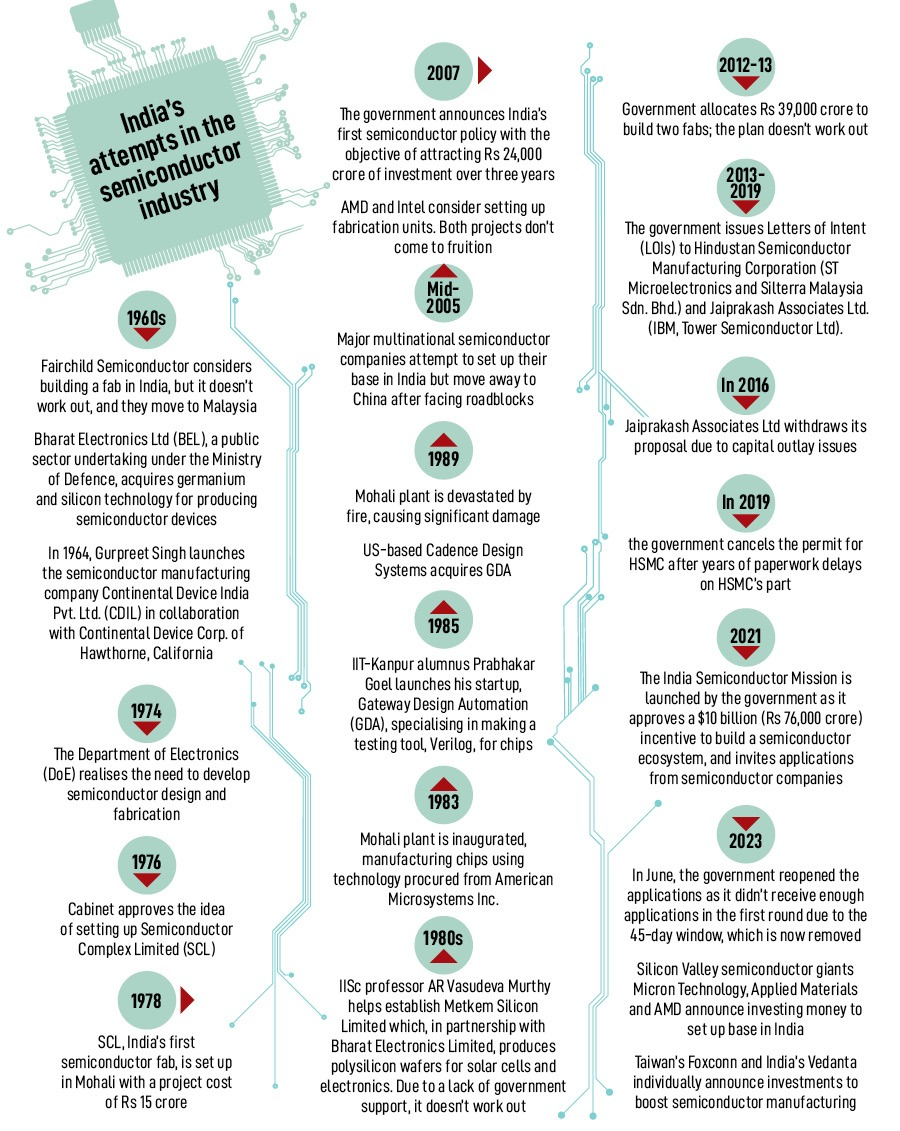
The mid-term evaluation of the Design-Linked Incentive (DLI) scheme, a crucial element of India's Semiconductor Mission, is approaching. Despite its goal of supporting 100 start-ups over five years, only seven have been approved, prompting a call for a reassessment and potential revamping of the scheme.
India aspires to become a global semiconductor hub, but the semiconductor chip shortage has underscored weaknesses in the supply chain, emphasising the urgency of enhancing domestic manufacturing capacity.
What are Semiconductors?
- Any of a class of crystalline solids intermediate in electrical conductivity between a conductor and an insulator.
- Semiconductors are employed in the manufacture of various kinds of electronic devices, including diodes, transistors, and Integrated Circuits (ICs). Such devices have found wide application because of their compactness, reliability, power efficiency, and low cost.
- As discrete components, they have found use in power devices, optical sensors, and light emitters, including solid-state lasers.
- Semiconductors are typically crystalline solids composed of atoms with four valence electrons. Silicon and germanium are two common elemental semiconductors used in electronic devices.
What is the India Semiconductor Mission (ISM)?
- About:
- The ISM was launched in 2021 with a total financial outlay of Rs. 76,000 crore under the aegis of the Ministry of Electronics and IT (MeitY).
- It is part of the comprehensive program for the development of sustainable semiconductor and display ecosystems in the country.
- The programme aims to provide financial support to companies investing in semiconductors, display manufacturing and design ecosystem.
- Envisioned to be led by global experts in the Semiconductor and Display industry, ISM will serve as the nodal agency for efficient, coherent and smooth implementation of the schemes.
- Components:
- Scheme for setting up of Semiconductor Fabs in India
- Scheme for setting up of Display Fabs in India
- Scheme for setting up of Compound Semiconductors / Silicon Photonics / Sensors Fab and Semiconductor Assembly, Testing, Marking and Packaging (ATMP) / OSAT facilities in India
- Design Linked Incentive (DLI) Scheme:
- About: It offers financial incentives, design infrastructure support across various stages of development and deployment of semiconductor design for Integrated Circuits (ICs), Chipsets, System on Chips (SoCs), Systems & IP Cores and semiconductor linked design.
- Nodal Agency: C-DAC (Centre for Development of Advanced Computing), a scientific society operating under MeitY, will serve as the nodal agency for implementation of the DLI scheme.
- 3 Components of DLI:
- Chip Design Infrastructure Support: Under this, C-DAC will set up the India Chip Centre to host the state-of-the-art design infrastructure (viz. EDA Tools, IP Cores and support for MPW (Multi Project Wafer fabrication) & post-silicon validation) and facilitate its access to supported companies.
- Product Design Linked Incentive: Under this, a reimbursement of up to 50% of the eligible expenditure subject to a ceiling of Rs.15 Crore per application will be provided as fiscal support to the approved applicants who are engaged in semiconductor design.
- Deployment Linked Incentive: Under this, an incentive of 6% to 4% of net sales turnover over 5 years subject to a ceiling of Rs.30 Crore per application will be provided to approved applicants whose semiconductor design for Integrated Circuits (ICs), Chipsets, System on Chips (SoCs), Systems & IP Cores and semiconductor linked design are deployed in electronic products.
- Vision:
- To build a vibrant semiconductor and display design and innovation ecosystem to enable India’s emergence as a global hub for electronics manufacturing and design.
- Significance:
- ISM is of paramount importance to organise efforts for promoting semiconductors and display industry in a more structured, focused, and comprehensive manner.
- It will formulate a comprehensive long-term strategy for developing semiconductors & display manufacturing facilities and semiconductor design ecosystem in the country.
- It will facilitate the adoption of trusted electronics through secure semiconductors and display supply chains, including raw materials, specialty chemicals, gases, and manufacturing equipment.
- It will enable a multi-fold growth of Indian semiconductor design industry by providing requisite support in the form of Electronic Design Automation (EDA) tools, foundry services and other suitable mechanisms for early-stage startups.
- It will also promote and facilitate indigenous Intellectual Property (IP) generation and encourage, enable and incentivize Transfer of Technologies (ToT).
- ISM will enable collaborations and partnership programs with national and international agencies, industries and institutions for catalysing collaborative research, commercialization and skill development.
What is the Overall Scenario of the Semiconductor Market?
- Global Scenario:
- The chip-making industry is a highly-concentrated one, with the big players being Taiwan, South Korea and the U.S. among others.
- Infact, 90% of 5 nm chips are mass-produced in Taiwan, by the Taiwan Semiconductor Manufacturing Company (TSMC).
- Therefore, the global chip shortage, U.S.-China tensions over Taiwan, and the supply chain blockages owing to the Russia-Ukraine conflict have led major economies to enter the chip-making sector with a renewed push.
- The global semiconductor industry is currently valued at USD 500-600 billion and caters to the global electronics industry currently valued at about USD 3 trillion.
- The chip-making industry is a highly-concentrated one, with the big players being Taiwan, South Korea and the U.S. among others.
- Indian Scenario:
- The Indian semiconductor market is valued at approximately USD 23.2 Bn and is projected to reach USD 150 Bn by 2029, growing at a CAGR of 27.10% during the forecast period.
- However, for the domestic manufacturing of semiconductor chips, India has recently launched several initiatives:
- To support semiconductor research and development (R&D) in India, MeitY has announced a USD 10 Bn investment in the ISM.
- India has also launched the Scheme for Promotion of Manufacturing of Electronic Components and Semiconductors (SPECS) for manufacturing of electronics components and semiconductors.
What are the Different Challenges in the Semiconductor Industry in India?
- Data Latency: Power, efficiency and task-based binning of wafer-die can lead to different co-products from the same wafer. Different tasks, each using varied planning parameters, triggers data latency issues since that data is stored in multiple disparate systems.
- Customer-Specific Needs: Often, the same product contains varied material, site, shipment size, and quality manufacturing. All such needs tend to vary as they are based on the customer's specific demands.
- Front-end (FE) Built Output: FE outputs such as wafers need further manufacturing steps such as assembly and testing as well as a blended model. This results in complexities across the supply chain, turning efficient capacity planning more difficult.
- Back-End (BE) Cycle Times Quicker than FE: The processing period of FE cycle is typically 6-8 weeks, whereas BE cycle times are mere 1-2 weeks only. This effectively means deferring inventory at different manufacturing periods, which needs additional planning.
- Restricted End-to-End Supply Chain Visibility and Planning: Abundant direct and indirect materials needed for manufacturing, and unrelated in-house and contractual manufacturing sites and distribution centres, makes supply chain prominence tough, learning to excess inventory growth and inefficient customer service.
- Extremely Expensive Fab Setup: A semiconductor fab can cost multiples of a billion dollars to set up even on a relatively small scale and lagging by a generation or two behind the latest in technology.
- High Investments Required: Semiconductors and display manufacturing is a very complex and technology-intensive sector involving huge capital investments, high risk, long gestation and payback periods, and rapid changes in technology, which require significant and sustained investments.
What are the Issues in the Implementation of DLI Scheme?
- While the DLI scheme aims to provide access to design infrastructure and financial subsidies, there is lacklustre uptake.
- Mandating start-ups to maintain domestic status and limiting foreign capital poses a significant barrier. The funding landscape and absence of a mature start-up ecosystem for hardware products in India reduce investor risk appetite.
- The semiconductor industry is highly competitive, with established players dominating the market.
- India would need to compete with countries like the US, S Korea, Taiwan, and China, which have well-established chip manufacturing industries.
- Gaining a competitive edge and attracting global investments in the face of such competition is a significant challenge.
- Intellectual property rights and licensing agreements play a crucial role in the semiconductor industry.
- Access to intellectual property, patents, and licences for advanced chip technologies can be a hurdle for India's chip making plans.
- Negotiating partnerships, licensing agreements, or developing indigenous intellectual property can be a complex process given the very low R&D expenditure compared to GDP.
How can ISM and its DLI Scheme be Overhauled?
- Integrating India's Semiconductor Strategy Goals:
- India's USD 10 billion Semicon India Program aims to reduce dependence on semiconductor imports, build supply chain resilience, and leverage its comparative advantage in chip design.
- The three goals involve strategic sectors, global value chain integration, and capitalising on India's existing design capabilities, which need to be integrated.
- Prioritising Investment for Maximum Benefit:
- With limited resources, industrial policy priorities should focus on maximising benefits. Stimulating the design ecosystem is less capital-intensive than foundry and assembly stages, creating strong forward linkages for India's semiconductor industry.
- Policy scrutiny should address the disparity in revisions between the DLI scheme and Production-Linked Incentive (PLI) schemes.
- Delinking Ownership from Development:
- The relatively modest incentives under the DLI scheme may not be a worthwhile trade-off for start-ups facing restrictions on ownership.
- Delinking ownership from semiconductor design development and adopting more start-up-friendly investment guidelines could enhance financial stability and provide global exposure.
- Broadening the Focus of the DLI Scheme:
- The primary aim of the DLI scheme should be to cultivate semiconductor design capabilities in India, fostering indigenous companies over time.
- The scheme needs to shift its focus to facilitate design capabilities for various chips within the country, regardless of the entity's registration, with a substantial increase in financial support.
- Establishing a Capable Institution for Policy Implementation:
- A recalibrated policy focused on chip design, led by a capable institution, can tolerate a certain failure rate and treat beneficiary start-ups as exploratory risk-taking vehicles.
- A revamped DLI scheme under the ISM, inspired by SFAL's approach, could attract a broader range of semiconductor design start-ups and help them overcome initial hurdles.
- Utilising Existing Facilities:
- Semiconductors and displays are the foundation of modern electronics driving the next phase of digital transformation under Industry 4.0.
- India’s Public Sector Enterprises (PSEs) such as Bharat Electronics Ltd or Hindustan Aeronautics Ltd can be used to set up a semiconductor fab foundry with the help of a global major.
- Collaboration:
- Though India is focusing on “lagging-edge” technology nodes in the start to supply to the automotive and appliance sector, creating global demand may be difficult as big players like Taiwan offer viable cutting-edge chip-tech worldwide.
- Besides the US and Japan, India should also explore similar opportunities to collaborate with other countries such as Taiwan, S Korea etc or other technologically advanced, friendly nations to promote domestic manufacturing and reduce import dependency in this sector.
Conclusion
The DLI scheme faces challenges such as restrictive ownership conditions, significant costs, and limited incentives, necessitating a shift in focus towards cultivating semiconductor design capabilities. Revisions should include delinking ownership from development, enhancing financial support, and reconsidering the role of the nodal agency. A recalibrated policy, guided by a capable institution, can tolerate some failure while establishing India's foothold in the high-tech semiconductor sector.
|
Drishti Mains Question: Discuss the challenges and policy recommendations for fostering growth in India's semiconductor industry, focusing on the Design-Linked Incentive scheme and potential reforms. |
UPSC Civil Services Examination, Previous Year Question (PYQ)
Prelims:
Q. Which one of the following laser types is used in a laser printer? (2008)
(a) Dye laser
(b) Gas laser
(c) Semiconductor laser
(d) Excimer laser
Ans: (c)
Q. With reference to solar power production in India, consider the following statements: (2018)
- India is the third largest in the world in the manufacture of silicon wafers used in photovoltaic units.
- The solar power tariffs are determined by the Solar Energy Corporation of India.
Which of the statements given above is/are correct?
(a) 1 only
(b) 2 only
(c) Both 1 and 2
(d) Neither 1 nor 2
Ans: (d)